A breakthrough materials mapping technique developed by UConn scientists has led to the discovery of highly-conductive properties in cadmium telluride, a promising material that could someday surpass the performance of silicon in solar cells.

While studying the effects of a chloride solution treatment on solar cells made of cadmium telluride, a team of researchers led by UConn UTC Professor of Engineering Innovation Bryan Huey noticed that microscopic “fault lines” within and between crystals in the material acted as conductive pathways that eased the flow of electric current.
Normally, such “planar defects” – the fault-like misalignments in the arrangement of atoms within a material – are viewed as a bad thing. They can create dead-end traps in materials that interrupt the flow of electric current in solar cells and reduce their efficiency. But just the opposite is true, it appears, with cadmium telluride.
“Cadmium telluride is a market-ready technology and primary competitor to silicon-based solar cells,” says Justin Luria, a Sunshot Postdoctoral Fellow in Huey’s lab and one of the UConn project’s lead researchers. “This study identifies new paths to optimize the performance of cadmium telluride solar cells and increases our understanding of the conductive properties of this promising material.”
The team’s findings appear today, in the Sept. 26, 2016 issue of the journal Nature Energy.
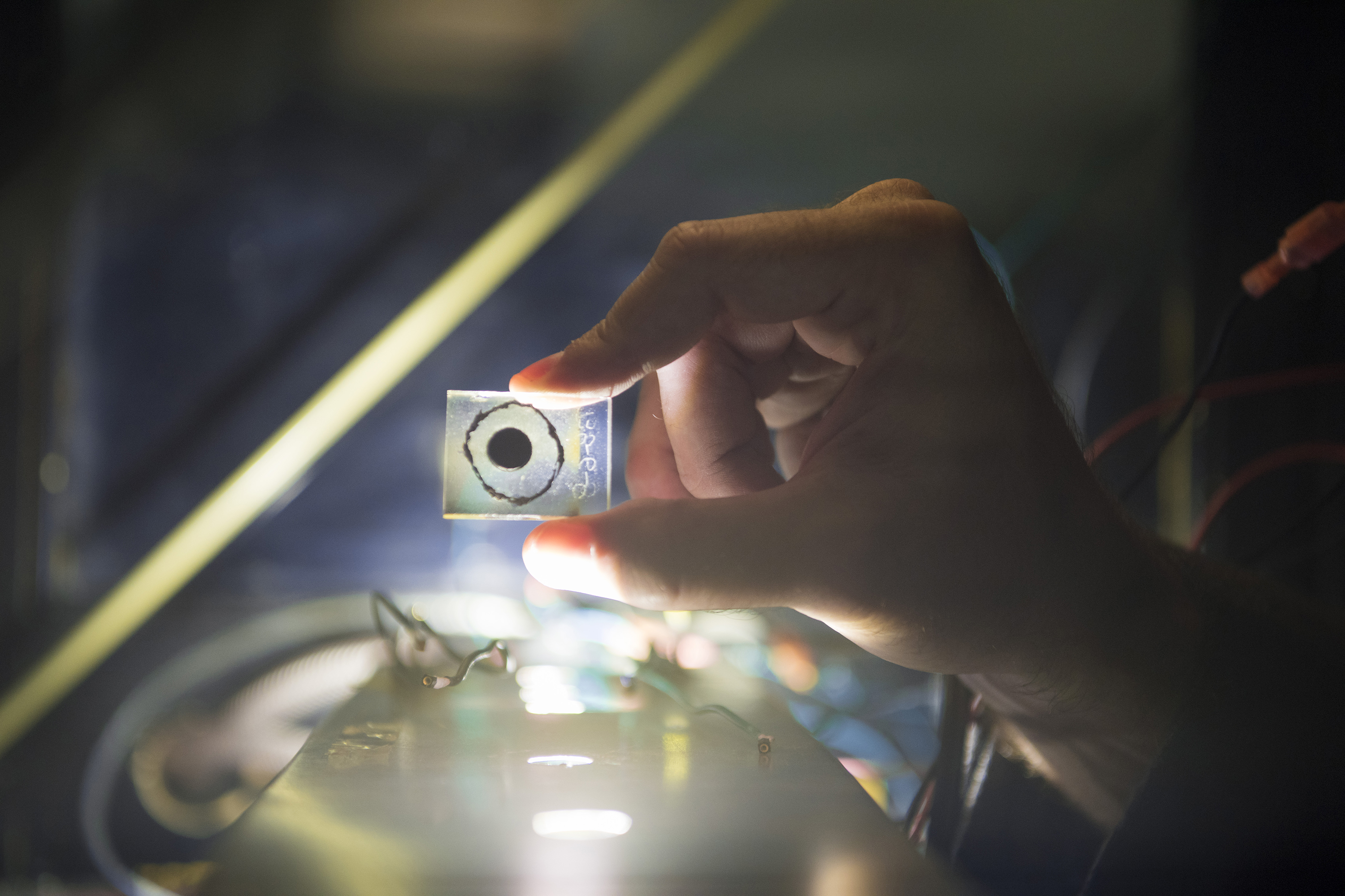
A novel materials mapping technique developed by Luria and UConn graduate student Yasemin Kutes led to the findings. Working in UConn’s Institute of Materials Science over the past two years, Luria and Kutes created an innovative microscopic mapping process that allowed them to capture hundreds of sequential images of the cadmium telluride as they peeled off one nanoscale layer at a time. The resulting data allowed the team to build a three-dimensional, high-resolution ‘tomographic’ map of a cadmium telluride solar cell, somewhat like what is created in medical science during a computed tomography (CT) brain scan, also known as a CAT scan.

Previously, scientists around the world have been limited when scanning surfaces or cross-sections of solar cells using traditional methods. UConn’s research marks the first time scientists have successfully gathered three-dimensional images of photo-electrical currents traveling beneath the surface of a solar cell.
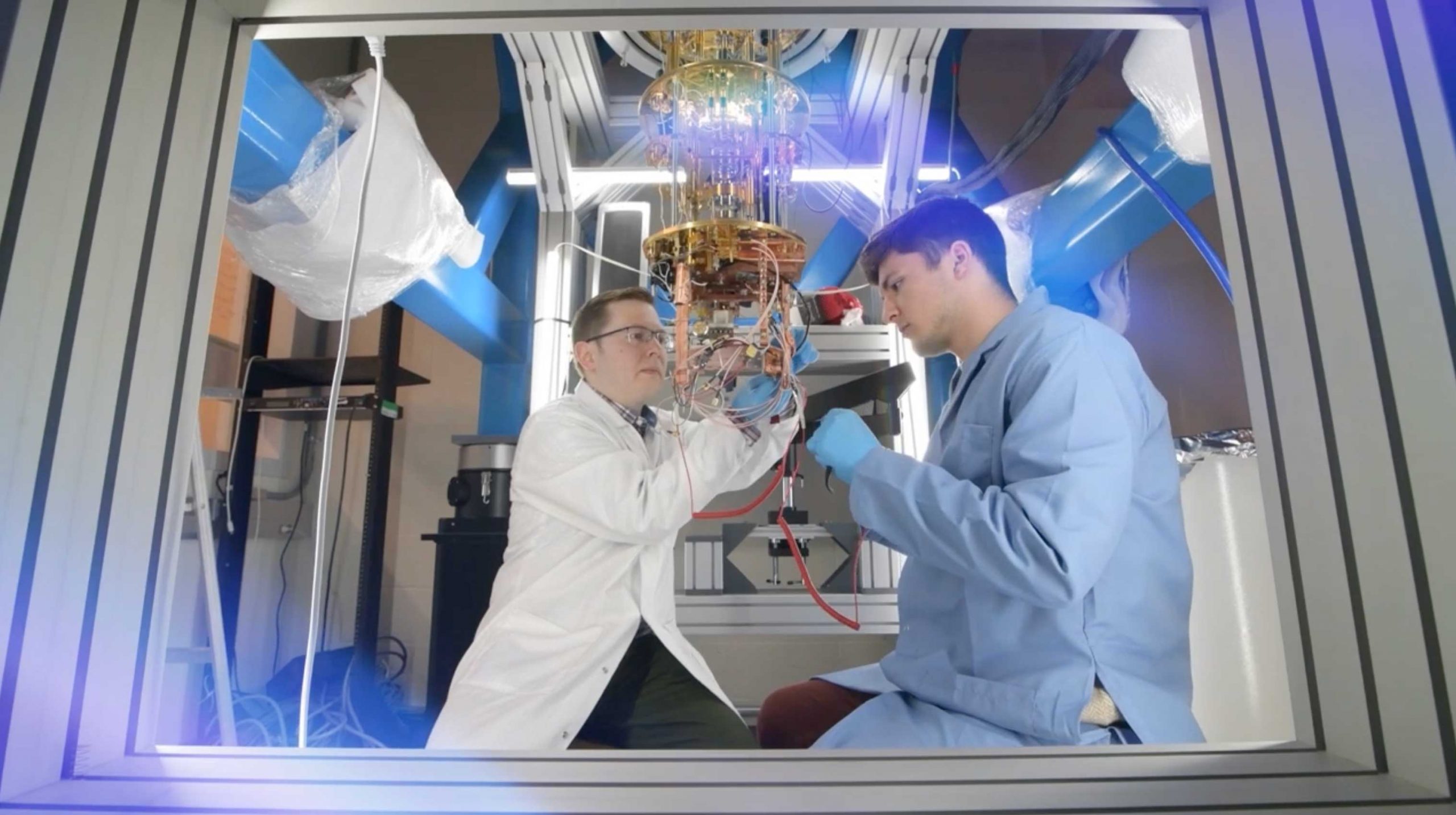
“Everyone using these microscopes basically takes pictures of the ‘ground,’ and interprets what is beneath,” says Huey, an associate professor of materials science and engineering. “It may look like there’s a cave, or a rock shelf, or a building foundation down there. Instead, we carefully dig, like archeologists, keeping track of exactly what we find every step of the way – though, of course, at a much, much smaller scale.”
The atomic force microscope (AFM) used by Huey’s group in UConn’s NanoMeasurements Lab applies a very fine probe, half a million times sharper than a pencil point, across a surface to track its topography – the hills and valleys of the surface structure. For this project, the researchers simultaneously measured the current induced by exposure to artificial sunlight, just as for an actual solar cell.
The resulting maps created by the UConn team revealed current flowing most freely along the crystal boundaries and fault-like planar defects. Samples of cadmium telluride that had been treated with the chlorine solution had more defects overall, a higher density of these defects, and what appeared to be a high degree of connectivity among them, while untreated samples had few defects, no evidence of connectivity, and much lower conductivity.

The team shared its findings with physicist Eric Stach, head of the electron microscopy group at the Brookhaven National Laboratory’s Center for Functional Nanomaterials (CFN), seeking to confirm its suspicions that the material’s defects were indeed caused by planar shifts in atomic alignments within the crystals. Advanced instrumentation at the CFN, a U.S. Department of Energy Office of Science User facility, would allow researchers there to take UConn’s work another step by analyzing the structure of the material at the atomic scale.
CFN staff physicist Lihua Zhang used a transmission electron microscope and UConn’s results as a guide to meticulously study how atomic-scale features of chloride-treated cadmium telluride related to the conductivity maps.
“When we looked at the regions with good conductivity, the planar defects linked from one crystal grain to another, forming continuous pathways of conductance through the entire thickness of the material,” says Zhang. “So the regions that had the best conductivity were the ones that had a high degree of connectivity among these defects.”
The advanced imaging process developed at UConn provides scientists a new systematic method that can be used to determine whether defects found in a material are good or bad in terms of conductivity, says Stach, who, with Zhang, serves as a co-author on the paper. It can also be used to explore the effects of different processing methods or chemicals to control how defects form.
“There is already a billion-dollar-a-year industry making cadmium telluride solar cells, and lots of work exploring other alternatives to silicon,” says Stach. “But all of these alternatives, because of their crystal structure, have a higher tendency to form defects … In the case of cadmium telluride, we may want to find ways to make more of these defects, or look for other materials in which defects improve performance.”
Either way, Stach says, combining the new computed tomography technique developed at UConn and electron microscopy yields a “clear winner” in the search for more efficient, cost-competitive alternatives to silicon solar cells.
This research was supported by the U.S. Department of Energy’s (DOE) Office of Energy Efficiency and Renewable Energy (EERE) – including its Sunshot Program – and the DOE Office of Science. The cadmium telluride samples were provided by Andrew Moore of Colorado State University.
For more information on the research, go to the Brookhaven Lab’s news site.