By: Eli Freund, Editorial Communications Manager, UConn School of Engineering
Solar panel technology has seemingly boomed over the last 20 years, but when you dig into the numbers, only six percent of U.S. homes have panels installed on their roofs. The prevailing material used in solar cells is silicon, which is easy to manufacture and lasts decades, but the cost has remained high. University of Connecticut Materials Science and Engineering Department Head Bryan Huey and his postdoc Jingfeng Song have produced some compelling research reported in the journal Nature Communications that could lead to another lesser-known material to come to market at a fraction of the price.
The material, known as Hybrid perovskites (HPs), can be manufactured into a thin film that is 200 times thinner than a conventional silicon cell but is just as efficient.
The biggest problem, says Huey, is their longevity doesn’t yet match silicon cells, which are the prevailing material used in solar cells.
“The primary limitation thus far is that their lifetime cannot yet compete with modern silicon cells, especially because the perovskites are highly sensitive to humidity. From an engineering perspective, that ought to be solvable—we also needed to figure out how to protect silicon from humidity, and now those panels can be warrantied to still produce 80% of their installed efficiency after 25 years. Current targets are for 50 years.” Huey said.
“Imagine any other technology being able to keep working so well after so long. If the perovskite thin films cells can survive even to just 5-10 years, they’ll begin to displace Silicon panels due to cost advantages.”
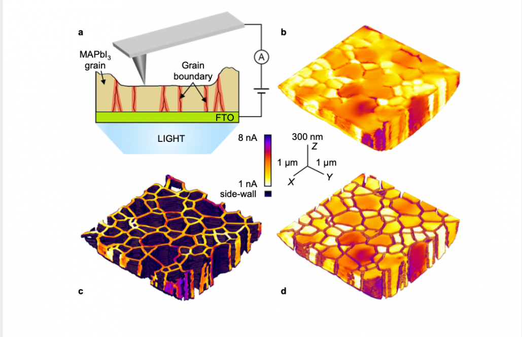
To help accelerate the technology to market, Huey and his team have spent the past several years developing a unique method of 3D mapping called tomographic atomic force microscopy (T-AFM). In this technique, which uses a super-hard tip to scrape away and map the layers of the material, researchers were able to study the grain boundaries of the material, which had previously only been studied at the surface.
Huey said that studying the grain boundaries beneath the initial surface allows scientists to understand the functionality of energy generation more accurately.
“Surprisingly, we found a new type of grain boundary, which is almost indistinguishable from the other interfaces at the top surface. After digging into the HP thin film, these interfaces behave as if there is no grain boundary at all. They don’t provide any particular advantage compared to the adjacent grains, and indeed photo-generated electron and holes carriers are almost free to travel across them, instead of channeling along them. Without our T-AFM advances at UConn, thanks to an NSF grant along with support from the SOE and IMS, we’d all still be guessing at what lies beneath the surface.”
With this new research out, Huey hopes that scientists and manufacturers use this new knowledge to make HP technology more accessible to the consumer. Next he hopes to turn his attention to another piece of the puzzle—solar cell degradation.
“Specific to Hybrid Perovskites, our results may guide the efforts of film manufacturing, and device design, to either leverage or suppress the properties of the 2 distinct grain boundary types we’ve resolved. While we continue to develop the method and apply it to several fundamental problems in materials science, we are also specifically focusing on solar cell degradation, one of the greatest remaining roadblocks for HP films before they can really compete in the >$100Billion solar panel market. Tune back again soon–we’re just beginning to scratch the surface.”
Professors Yuanyuan Zhou and Nitin Padture from the School of Engineering at Brown University, who collaborated with the team at UConn on this research, said that these findings can have a ripple effect on the industry.
“The tomographic AFM technique has the unique capability of revealing 3D buried microstructures at the nanoscale during perovskite device operation and degradation. This is extremely helpful for scientists and engineers to develop more robust hybrid perovskites devices in the future.” Said Zhou and Padture.
The team received support from the National Science Foundation (MRI development award, DMR-1726862), and the Institute of Materials Science of UConn.